
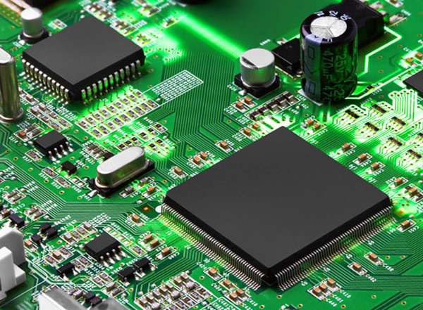
Transistors are indeed one of the revolutionary inventions that man has ever made. The function of the transistor is to switch and amplify electrical currents. The number of transistors in dense integrated circuit doubles about every two years. This is Moore’s law.
In today’s post, I will introduce you to the semiconductor world and will explain the working of a transistor which has revolutionized our world. Without transistors, today’s electronics and gadgets wouldn’t have existed.
To understand how transistors work we need to learn basics. Let’s first understand a diode. A diode is a semiconductor device which allows a unidirectional flow of current. A diode has two terminals and is made from two types of a semiconductor; p-type and n-type.
P-TYPE SEMICONDUCTOR:
When a semiconductor like silicon is doped with trivalent impurity like Indium, Boron, Aluminium, etc. we get a p-type semiconductor. This is because silicon has four electrons in their valence shell or valence band and the trivalent impurity has only three valence electrons. This results in having a vacant space on the doped atom which we called a hole.
While talking about p-type semiconductor we like to talk about majority charge carriers which in this case are holes or can also say positive charges since they are missing negative charges and showing attraction towards negative terminal.
N-TYPE SEMICONDUCTOR:
When a semiconductor like silicon is doped with pentavalent impurity Arsenic, Antimony, Phosphorous, etc. we get an n-type semiconductor. This is because silicon has four valence electrons and pentavalent impurity has five valence electrons leading to having an extra electron that goes into the conduction band. The net charges of p-type and n-type semiconductors are neutral.
P-N DIODE:
When we connect these two types of semiconductors we get a p-n diode. At the boundary where these two semiconductors are joined, show some exciting behavior. This boundary is called p-n junction and at this p-n junction, the majority charge carriers of the respective semiconductors cross the boundary and form a depletion layer. Now here’s the main part; when we connect negative terminal to p-type semiconductor and positive terminal to n-type semiconductor, no current passes through the circuit, this type of connection is called reverse bias. Whereas when we connect positive terminal to p-type and negative terminal to n-type the depletion layer decreases and the current starts flowing. In this situation the circuit behaves like a closed switch and such a connection is called forward bias.
WORKING OF A TRANSISTOR:
Now let’s look after transistors; instead of two, transistors have three layers each doped with different densities. The three layers or terminals are the emitter, the base, and the collector respectively.
The emitter is highly doped, the base is very thin and lightly doped whereas the collector occupies a large region with medially doped. There are two types of transistors; n-p-n type and p-n-p type. Today we will be considering the n-p-n type of transistor. Here’s how the circuit looks like:
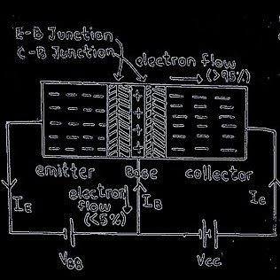
From the above diagram, we can say that emitter-base (E-B) junction will act as a forward bias whereas base-collector (B-C) junction will act as reverse bias i.e. current will flow from E-B junction but not from B-C junction. But that’s not what happens in the case of transistors.
Since the base is very thin, almost 95% of electrons from the emitter go to the collector and then to the positive terminal and only 5% current flow through the base. Thus a small change base will lead to maximum current flow from the collector i.e. a kind of amplifying the current. Remember Moore’s law I initially talked about? It’s estimated that by 2025 we will reach a limit when transistors will be so small that quantum effects will take over and the electrons will easily pass the barrier without electrical potential via quantum tunneling. Thus scientists are developing molecular and quantum transistors. I will be talking about quantum computation and working of quantum computers in my future post, so stay tuned and subscribe to the blog to get the latest post notification.


Greetings! Very helpful advice on this article! It is the little changes that make the biggest changes. Thanks a lot for sharing!